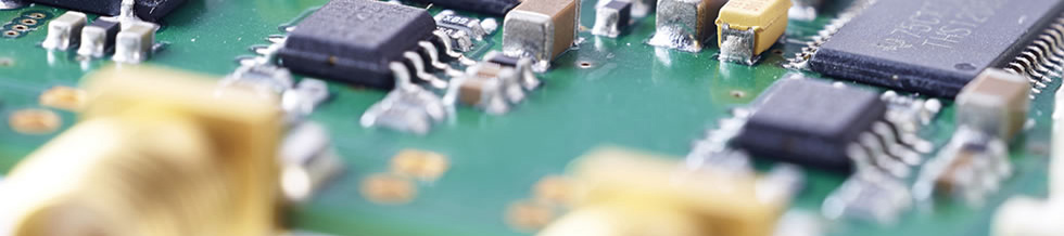

UniDAQ Prozessor-Board UniDAQ2.DSP-ADDA
Das UniDAQ2 ist ein vielseitiges Datenerfassungs- und Signalverarbeitungs-System für industrielle Anwendungen, wissenschaftliche Forschung und Ausbildung.
16 simultan abgetastete analoge Eingänge mit exzellenter Performance und geringer Latenzzeit qualifizieren das UniDAQ2 für die hochgenaue Messung dynamischer Signale und für Regelungen. 8 Analogausgänge steuern Aktoren, generieren Stimuli, Referenzspannungen oder können zur Überwachung interner Verarbeitungszustände verwendet werden.
Typische Einsatzgebiete
- Schwingungsanalyse und Maschinen-Überwachung
- akustische Signalauswertung, Mikrofon-Array Messtechnik
- Regler und Positioniersysteme
- Messsysteme für Forschung, Entwicklung und Prüfstände
- Laborausrüstung für die Ausbildung in Signalverarbeitung und Mechatronik
Software
- Web-Frontend für einen schnellen Einstieg in die Bedienung, Konfiguration und Visualisierung Ihrer Daten
- Direkter Zugriff über Matlab® Instrument Control Toolbox, Python oder C Programme auf dem PC durch TCP/IP-Protokollschnittstelle
- DSP-Bibliothek zur Unterstützung Ihrer Gerätekonfiguration, Datenerfassung und Kommunikation
- Treiber für TCP/IP, USB-CDC, USB-TMC und USB-DFU
Key Features
- 16 simultan abtastende SAR A/D-Wandler, 16-bit, 175kS/s
- 8 inhärent monotone D/A-Wandler, 16-bit, 105kS/s
- interne oder externe Abtasttakt-Generierung für ADC und DAC
- 456 MHz Fliesskomma DSP (TMS320C6747) mit 64 Mbyte SDRAM
- USB2.0 Device Port und 100Base-T Fast Ethernet
- Erweiterungsport für Massenspeicher, Feldbus-Anbindung, Display, GPIOs
- isolierter Analogteil
- nur eine Stromversorgung 5-18V, ca. 3W

Input Characteristics
| Number of Channels | 16 single-ended (8 differential), simultaneous sampling |
| ADC Resolution | 16 bits |
| Type of ADC | Successive approximation register (SAR) |
| Sampling Rate | 0 - 175 kS/s, internal or external sampling clock |
| Input Range | ±5 V and ±10 V, programmable |
| Input Coupling | DC |
| Input Impedance | 1 MOhm || 10pF |
| Input Leakage | 1.5µA typ. |
| Overvoltage Protection | ±36 V, Input current during overvoltage conditions max ±10mA |
| Antialias Filter | 2nd order Butterworth, -3dB cutoff 15 kHz (±5V Range), 23 kHz (±10V Range) |
| DNL | ±0.5 LSB typ, < ±1 LSB max |
| INL | ±0.5 LSB typ, ±2 LSB max |
| Zero Error | < 2 mV |
| Full Scale Error | < 0.3% |
| Channel to channel | |
| Phase Mismatch | <0.1° at 1kHz, <0.5° at 10kHz input frequency |
| Crosstalk | -115dB to adjacent channel, 10kHz full-scale input signal |
| Latency | 6 µs from sampling clock to ADC1,5,9,13 data available in DSP 10µs until all ADC channels are available in DSP |
| Dynamic Characteristics | (input 1kHz sine, -1dB full scale, 100kS/s, no oversampling) |
| SINAD | 87 dB |
| THD | -100 dB |
| SFDR | 108 dB |
Output Characteristics
| Number of Channels | 8 single-ended, simultaneous sampling or single-DAC update mode |
| DAC Resolution | 16 bits |
| Type of DAC | String DAC, inherently monotonic |
| Sampling Rate | 0 - 105 kS/s, internal or external sampling clock. Simultaneous sampling synchronized to ADC or triggered by an independent clock source. |
| Settling Time | full scale step: 10us to 0.03%, 15us to 1LSB |
| Output Range | ±5 V and ±10 V, programmable unipolar and asymmetric output range by programming the DAC offset register. Gain and zero calibration registers per channel. |
| Startup Voltage | 0V |
| Output Coupling | DC |
| Output Impedance | 50 Ohms |
| Current Drive | ±5mA, short-circuit limited to 70mA |
| Capacitive Drive | 20000pF |
| Antialias Filter | 2nd order Butterworth, -3dB at 50kHz |
| DNL | ±0.5 LSB typ, ±1 LSB max |
| INL | ±1.5 LSB typ, ±4 LSB max |
| Zero Error | < 3 mV uncalibrated |
| Full Scale Error | < 0.3% uncalibrated |
| Crosstalk | -105dB to adjacent channel, 10kHz full-scale output signal |
| Dynamic Characteristics | (output 1kHz sine, -1dB full scale, 100kS/s) |
| SINAD | 74 dB |
| THD | -74 dB |
| SFDR | 75 dB |
Trigger Inputs
| Number of Channels | 2 |
| Input Range | 3.3V and 5V TTL/CMOS compatible, Overvoltage Protection: ±36 V, Input current during overvoltage conditions max ±10mA |
| Usage | ADC conversion start DAC update Pre- or post trigger event to DSP and/or Expansion Board Capture inputs (frequency, pulse width, duty cycle) Quadrature input (relative rotation angle and speed) |
Trigger Outputs
| Number of Channels | 1 |
| Output Range | 3.3V LVTTL, 5V TTL/CMOS compatible |
| Output Impedance | 50 Ohms |
| Usage | ADC sampling clock output Trigger event or clock output from DSP and/or Expansion Board |
Communication Ports
| Ethernet | 1 Port, 100 MBit/s, full-duplex, RJ45 |
| USB2.0 | 1 Port, 480 MBit/s, Typ B (device) |
Signal Processing
| DSP | Texas Instruments TMS320C6747, 456 MHz, optional: OMAP-L137 DSP + ARM9 |
| Memory | 32 Kbytes L1 Program RAM/Cache 32 Kbytes L1 Data RAM/Cache 256 Kbytes L2 RAM/Cache 128 Kbytes L3 RAM 64 Mbytes SDRAM, 133 MHz 8 Mbytes non-volatile Flash Memory |
Debugging Ports
| JTAG | TI in-circuit emulator, 14-pin header, 2.54mm pitch |
| Debug UART | 1 x RS232, TxD and RxD, 3pin KK-connector 2.54mm pitch |
Expansion Port
| Connector | 80-pin, 0.8mm pitch |
| Signals | DSP EMIFA * (asynchronous parallel bus and NAND-Flash support) DSP UHPI * (parallel host processor interface) DSP SD/MMC * (eMMC or SD-Card expansion) DSP LCDC * (LCD Controller) * These signals share the same pins. With the exception of the LCD + SD/MMC combination, usage is mutually exclusive. 4 x GPIO, unused signals of the above interfaces can be used as additional GPIO 1 x SPI 1 x I2C Trigger Signals (2 x in, 3 x out) Power Supply 3.3V and VIN (5 to 18V) |
Power Supply
| Supply Voltage | 5 - 18V ±5%, reverse-polarity protected |
| Power Consumption | 3W typical |
Isolation
| max. Voltage | 350VAC / 500VDC between analog GND and digital GND / power supply |
Mechanics
| Size | Eurocard, 160 x 100 x 15 mm |
Operating Conditions
| Ambient Temperature | 0-70°C |
| Humidity | max. 95% rel., non condensing |
| UniDAQ2.DSP-ADDA | Standard-Board |
| DSW.UniDAQ | Softwareentwicklungsunterstützung für UniDAQ und kostenfreiem Support per Telefon und Email |
| DK.UniDAQ2 | Entwicklungskomplettpaket UniDAQ2.DSP-ADDA inklusive Board und kostenfreiem Support per Telefon und Email |
| DS.TCPIP-UniDAQ2 | Ethernet Entwicklungs-Basispaket |
| UniDAQ.EXP1 | UniDAQ Erweiterungskarte zum Anschluss eines LCD-Displays, SD-Kartensteckplatz, batteriegepufferte Echtzeituhr |
| DK.UniDAQ.EXP1 | Entwicklungspaket für UniDAQ.EXT1 inklusive LCD-Display, Support CD, FAT Filesystem und kostenfreiem Support per Telefon und Email |
- UniDAQ2.DSP-ADDA bestückt mit OMAP-L137 (DSP C6747 + ARM9) statt TMS320C6747 DSP
- UniDAQ3.DSP-ADDA: UniDAQ2.DSP-ADDA bestückt mit 24bit Sigma-Delta-Wandlern statt 16bit SAR-Wandlern erreichen eine Mess-Bandbreite von 100kHz bei simultaner Abtastung aller Kanäle
- UniDAQ.EXP1: LCD-Display und Touchscreen Interface, SD-Kartensteckplatz und batteriegepufferte Echtzeit-Uhr
D.SignT verfügt durch viele Projekte im Messtechnikbereich über umfangreiche Erfahrung im Analogdesign. Somit können kundenspezifische Analog-Frontends für das UniDAQ-System von D.SignT in kurzer Zeit umgesetzt werden.
Wie zum Beispiel:
- 8 differentielle oder 16 single-ended Spannungseingänge mit PGA,
8 Speisespannungen/-ströme für Sensoren oder - 8 Brückeneingänge, Shunt-Kalibrierung, Halbbrückenergänzung,
TEDS, Brückenspeisung oder - 8 Eingänge für Piezo-Beschleunigungs-Aufnehmer mit IEPE und TEDS oder
- 8 Mikrofon-Eingänge, PGA, TEDS, Stromquellen für CCP, ICP, IEPE, CCLD usw.
Emulatoren
Compiler
TCP/IP Stack